Although Samsung delivered the first commercial chip using the 3 nm process as well as the new “gate all around” transistor architecture, this does not guarantee its lead over TSMC.
For the delivery of its first 3 nm chips using GAAFET technology, Samsung organized a ceremony in its Korean factories, bringing together politicians, senior company officials and partner companies. On paper, this pomp is justified: Samsung Electronics is making industrial history by being the first to deliver commercial processors that are as thin (TSMC only delivers 4 nm) and as modern.
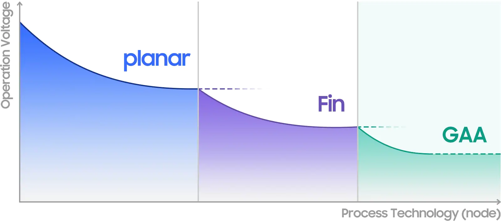
After a decade dominated by finned field-effect transistors – FinFET in jargon – the world of semiconductors is taking a new turn with a new structure: the Gate All Around Field-Effect Transistor or GAAFET (MBCFET for Multi-Bridge Channel Field-Effect Transistor for Samsung’s proprietary name). This “gate” which completely “surrounds” the transistor, indeed offers a very important field of improvement for the future of our chips. Processor designers will be able to play more finely on voltages (many more levels), increase frequencies and reduce energy consumption.

Delivering a chip that is ahead on two counts – manufacturing and transistor design – seems to guarantee Samsung a weighty advantage, especially against TSMC and Intel who are developing the same technologies. Nope ? No. Because if being late can be catastrophic in the field of semiconductors, being a little too early is not desirable either. And above all, there is a rather cruel precedent for Samsung: EUV engraving.
Samsung first on the EUV, and quickly overtaken by TSMC

In December 2020, Qualcomm announced that it would switch from TSMC to Samsung for the engraving of its flagship processor at the time, the Snapdragon 888. A chip engraved in 5 nm which would be replaced the following year by the Snapdragon 8 Gen 1, also engraved by Samsung. Two chips certainly powerful, but whose integration in high-end Android terminals is tainted by concerns of overheating. Design issues? If the question arose at the beginning of the Snapdragon 888 story, a recent chip has just set the record straight: the Snapdragon 8+ Gen 1.
The little “+” usually means small production optimizations that grant a few percentage points more performance. But this year, the “+” version has the major modification of switching from Samsung 4 nm 4LPE engraving to TSMC’s 4 nm (4N process). A constant dimension foundry change (4 nm) which sounds like a cold shower for Samsung: compared to the “normal” Snapdragon 8 Gen 1, the “+” version is more efficient (sometimes beyond 10%!) by heating less and consuming less energy.
However, on paper, Samsung had the advantage of technological leadership, since it was in April 2018 that Samsung proudly announced that it was the first to deliver the first commercial chips etched in extreme ultraviolet (EUV). It is this technology that has enabled manufacturers to overcome the 7 nm “wall”, the first fineness of engraving where EUV has proven necessary to avoid excessively high waste rates. Beyond 7 nm, EUV is even absolutely mandatory to continue reducing the size of circuits.
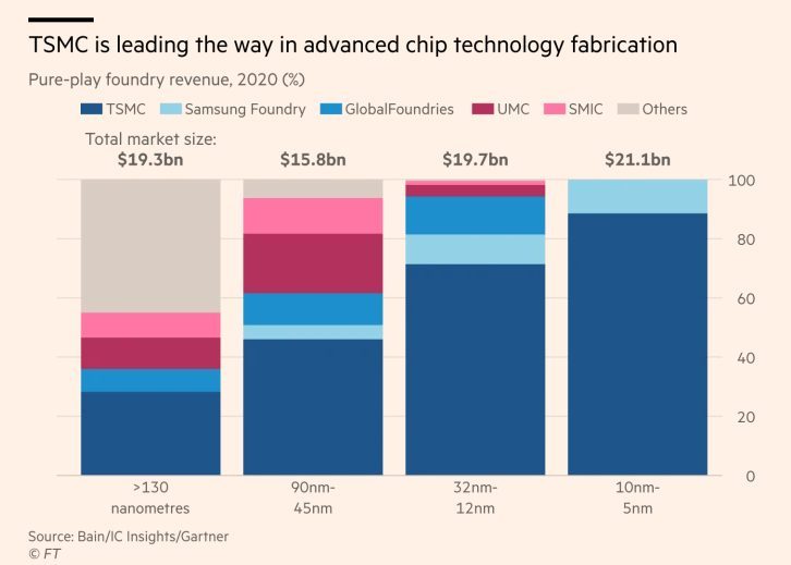
Even though Samsung was the first to commercially deploy EUV, it is TSMC that carves out the lion’s share of the world’s production of advanced chips using this technology: 90% of these chips are produced by the Taiwanese and only 10% are by Samsung. With, as shown by the example of Qualcomm’s Snapdragon 8(+) Gen 1, a decisive technological advantage for TSMC with an equivalent process…
Does this mean that Samsung will not succeed in taking the advantage this time around? Hard to say. We will have to wait to see the implementations of TSMC and Intel, who are also investing in the same technologies, to see which of the three titans has the best mastery of these two processes.
Thz Korea Herald
[related_posts_by_tax taxonomies=”post_tag”]
The post Chips engraved in 3 nm: why Samsung’s lead is not so decisive appeared first on Gamingsym.
